Bare Conductive and Printed Electronics: Advantages and Applications

At its heart, Bare Conductive is a printed electronics company operating in an industry with exciting innovations
Printed electronics: an overview
The term printed electronics was first coined in the 1940’s when an Austrian engineer named Paul Eisler realised that traditional printing technology could be applied to the manufacture of a Printed Circuit Board (PCB) to make printed circuits. However, the concept is believed to have been invented much earlier by a German named Albert Hanson, who filed a patent for “Printed Wires” in 1903. His idea involved gluing a circuit pattern cut from copper foil onto a paraffin paper substrate.
Printed electronics have come a long way since their conception over a century ago. Today, the term encompasses an entire industry devoted to the development of electronic devices and materials that incorporate this technology. It is also used to describe the printing methods used to manufacture the technologies themselves. According to IDTechEx, the Printed Electronics market is currently worth around $41.2B USD, it is estimated that it will be worth approximately $74B USD by 2030.
Printed electronics were originally used to create conventional electronics such as keyboards and antennas. As printing technology has evolved, along with the ability to print onto different substrates such as glass, paper and plastic, the field has expanded to include flexible and wearable electronics. Common applications for the technology include solar cells, touch screens and oled displays, near field communication (NFC) and printed RFID tags.
The Printed Electronics market is segmented by applications into the following categories: lighting, batteries, RFID Tags, displays, photovoltaic (PV) cells, and sensors. With applications ranging from retail and packaging, to consumer electronics, aerospace, construction, automotive, and healthcare. According to a report by MarketsandMarkets a key area of growth is being driven by the Internet of Things (IoT), where printed electronics will play a critical role in the integration of smart surfaces and smart materials into the built environment.
How do printed electronics work?
Printed and flexible electronics are created by applying a solution-based conductive material onto a substrate using printing equipment. Low cost processes used in traditional printing such as inkjet printing, screen printing, flexography, gravure printing, and offset lithography are used to create electrical devices. Nearly all industrial printing methods can be used for the manufacture of printed electronics. Printing technologies divide between sheet-based and roll-to-roll-based approaches. Sheet-based inkjet and screen printing are best for low-volume, high-precision work. Gravure, offset and flexographic printing are more common for high-volume production, such as photovoltaic cells. According to a market analysis report by Grand View Research, screen printing makes up over 50% of the revenue for the printed electronics industry.
To create a printed electronic device, electrically functional, electronic or optical inks are deposited on a substrate, creating active or passive devices, such as coils, resistors or capacitors. The materials applied include inorganic and organic semiconductors, metallic conductors, nanoparticles, or carbon nanotubes.
Depending on the use-case, printed circuits can be used to store a charge (sensor or battery), emit light when electricity is applied (OLED display), convert sunlight into electricity (solar cell), or numerous other applications.
What are flexible electronics?
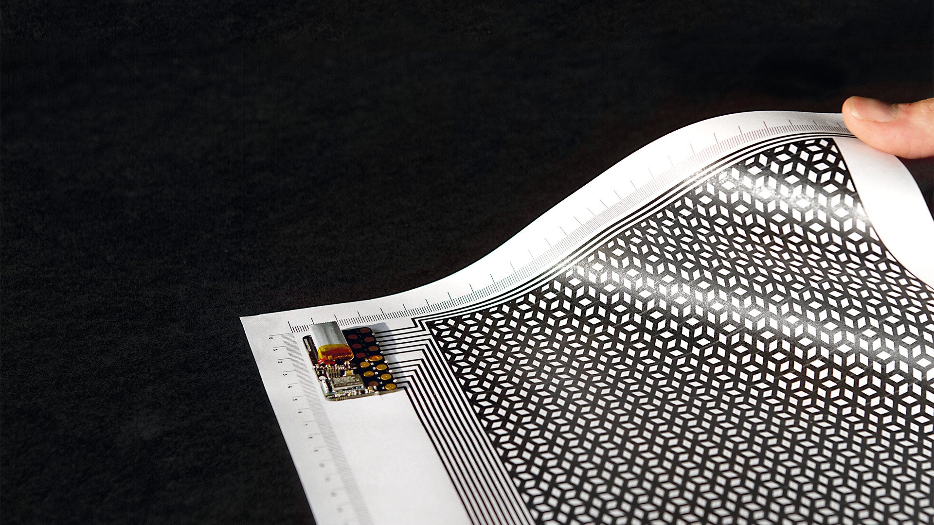
Traditional printed electronics are usually made on inflexible substrates. Flexible printed electronics are distinct from these in that they can fold, bend, twist, wrap, roll and stretch, conforming to many shapes and enabling the development of unique products, features and capabilities. A flexible circuit can be made up of several layers, but generally contains at least a passive flexible substrate made of plastic, paper or a textile, and conductive layer of conductive ink or foil. The conductive material used depends on the printing technique, but will usually be either graphene, silver, carbon, gold, or a composite of these.

(photograph by U.S. Army RDECOM / CC-BY-2.0 via Wikimedia Commons)
Advances in flexible electronics are revolutionizing the printed electronics industry. With their ability to conform to more organic shapes, they impart a degree of design freedom that can increasingly be incorporated into both consumer and industrial products. We can already see this in products that incorporate flexible displays, like LG’s rollable OLED tv, and flexible sensors, however that is only half the advantage. Thin, lightweight and low cost, flexible electronics also enable the integration of digital intelligence into a wide range of surfaces and materials. One can imagine a not-so-distant future where a flexible sensor integrated into a wall could enable the collection of data directly from our environment, bringing digital intelligence to our world, and making all our environments safer, healthier and smarter.
How is printed electronics technology designed?
The printed electronics industry is continuously evolving. New materials, processes, equipment and designs are constantly being developed to transform ideas into real products. In this ever-changing environment, industries that have not traditionally been associated with electronics are being disrupted, offering a wide opportunity for innovation and growth. This is only fitting, seeing as the field of printed electronics was invented in this way, by combining traditional techniques from the printing industry with electronics. Similar to conventional printing, printed electronics applies ink layers one atop another. So the coherent development of printing methods and ink materials are one of the field’s essential tasks.

(photograph by Bystrikt / CC-BY-SA-3.0 via Wikimedia Commons)
There are a few main areas where key advances in printed electronics are happening. Research and development focuses on the improvement of printing processes and equipment, development of materials with particular properties, design and integration of hardware, and software development.
Printed electronics technology is designed by making changes or innovations to each, or several of these features in conjunction to solve new problems, or by adapting these to meet particular product specifications. One of the reasons the printed electronics market can be slow to innovate, is that developing novel technology can require collaboration between different stages of the supply chain or technology stack, for example the paint chemistry or hardware development.
This presents a unique opportunity for companies such as Bare Conductive. Our focus on Dynamically Functional Surfaces as a complete solution makes us uniquely suited to address market needs from the bottom up, delivering complete outcomes that encompass material selection, sensor and hardware and industrial design, all the way to software development and connection to the cloud.
The challenges facing printed electronics
At Bare Conductive we believe the most interesting opportunity for printed electronics today is in the creation of smart buildings through the integration of printed circuits, flexible displays, sensors, and other electronic components into the built environment. However, there are many challenges to seamlessly integrating printed electronics into industry standard functional materials such as drywall, wallpaper, flooring and roofing.
Some of the challenges associated with these applications include substrate and material selection, paint deposition, printing patterns, hardware integration and software development. There are many things to consider when designing solutions around all these factors. For example:
Substrate and conductive ink – Developing solutions for smart buildings requires leveraging standard manufacturing processes and materials to take ad existing supply chains and minimize cost. Because of this, when selecting conductive coatings it is critical to select materials that make use of an existing printing method. The challenge lies in understanding what materials and manufacturing processes are best suited for standardizing the manufacture of smart building materials.
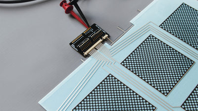
Printing patterns – When designing printed electronics, pattern design is a critical factor. For example, when designing touch sensors, the shape, size and pattern of a conductive trace can influence anything from material cost, to electrical interference, or a surface’s sensitivity and ability to perform a particular function. The challenge lies in developing the most effective pattern for a particular use-case or environment.
Hardware integration – Hardware is full of challenging opportunities for printed electronics. These range from the development of small or flexible electronic components that can be easily incorporated into printed electronic devices, to the design and manufacture of connectors that enable a robust and reliable link between rigid hardware and a flexible substrate.
Software development – Although not relevant for all printed electronics applications, when dealing with sensors and IoT devices which need to connect to building management systems or to the cloud, developing software becomes a critical part for ensuring a robust printed electronics stack.
Another challenge facing printed electronics is the lack of awareness of the applications and benefits these technologies can bring to fields not traditionally associated with electronics, and how these technologies can be harnessed and integrated into existing manufacturing processes.
This is where Bare Conductive leverages it’s broad community of individual users. By commercializing development kits, and making our technology accessible to designers, engineers and creatives, we put printed electronics in the hands of the broadest possible audience, stimulating an open channel for experimentation and exploration.
Printed electronics market and technology benefits
The end-use markets for printed electronics include automotive and transportation, consumer electronics, healthcare, retail and packaging, aerospace and defense, construction and architecture.
For most of these markets, the attraction of printing technology for the fabrication and integration of electronic components mainly comes from the possibility of preparing stacks of micro-structured layers in a much simpler and cost-effective way compared to conventional electronics.
These thin and flexible devices can facilitate widespread low-cost electronics for applications such as smart surfaces with integrated interfaces and switches, inbuilt occupancy sensors, discrete water sensors, flexible displays, smart labels, interactive walls, and active clothing and wearables.
Printing enables low-cost manufacturing at large scale, like in RFID-systems which enable contactless identification in trade and transport. Printing on flexible substrates allows electronics to be placed on curved surfaces, for example, printing solar cells on vehicle roofs, or the integration of buttons and switches into one part, such as a vehicle door, reducing cost in materials, assembly and part count. In some cases although cost is not lowered, like with conventional semiconductors, the higher cost is justified through much higher performance. Printed electronics allows the use of flexible substrates, which lowers production costs and allows fabrication of mechanically flexible circuits.
In the health sector, besides the development of non-intrusive wearables and monitoring devices, printed electronics has the potential improve health outcomes by tackling hygiene, infection and transmission. Printed electronics offer the ability to create integrated touch-less interfaces using hygienic materials, allowing for the design of surfaces such as keypads, controls or light switches which can be easily cleaned and disinfected. Manufacturing these switches directly into furniture or walls, can also enable monitoring of occupancy and cleaning events.
According to IDTechEx some of the many benefits of printed electronics technologies include:
- Lower costs
- Improved performance
- Flexibility
- Transparency
- Reliability
- Improved environmental impact and energy savings
Printed electronics applications, today and into the future
The most common applications of printed electronics technology today is in solar cells or photovoltaic panels for producing solar power, radio-frequency Identification (RFID) Tags and Antennas for tracking , monitoring devices, memory devices for data storage, OLED display screens, wearables, lighting or light-emitting diodes (LEDs), batteries and sensors.
Many of these applications have been around for decades, and as such continue to see incremental improvements through cost reduction and efficiency gains. To the general observer, the most obvious improvements are experienced through cheaper, thinner, higher quality consumer electronics devices (such as OLED screens). However, some areas are seeing dramatic changes as new manufacturing methods and technology advancements are leading to profound innovations that will change our world dramatically.
The integration of sensors into smart materials is one such area which will bring about a complete revolution to the built environment. The ability to print, and manufacture electronics directly onto construction materials is quickly becoming a reality, bringing us one step closer to a fully integrated Internet of Things.
At Bare Conductive we are working closely with some of the world’s largest companies in materials, construction, furniture, and transportation to integrate our sensor technology into the materials and surfaces that surround us. Just like tablet computers transformed books from a single function paper surface to a multi-use, multi-function platform through software and cloud connectivity, printed electronics have the potential to transform the walls and surfaces around us into active interfaces with a range of capabilities.
For more information on how we work with industrial partners to develop scalable printed electronics solutions make sure to visit the LAIIER.
Bare Conductive has launched LAIIER, productizing its Dynamically Functional Surface™ technology for applications in the smart building.
Stay connected with Bare Conductive. Follow, like and comment on Facebook, Twitter & Instagram.